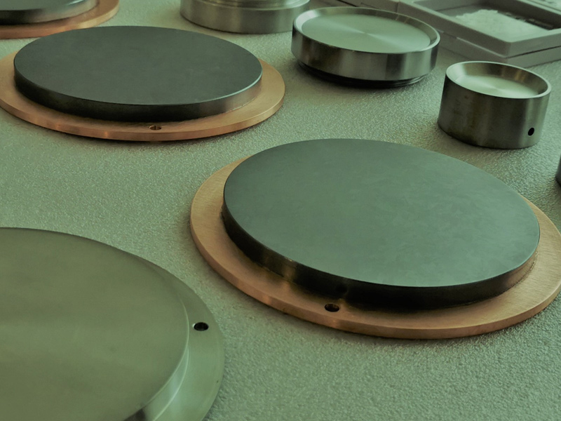
99.9% Crystalline Boron fraction in Semiconductor Sputtering Alloy Targets
99.9% crystalline boron fraction serve as solid-phase raw materials for alloy targets. Unlike amorphous boron powder, crystalline boron features an ordered structure, lower impurity levels, and superior thermal stability. Its key functions are as follows:
1. P-type dopant source for precise carrier concentration control
As a Group III element, crystalline boron acts as a substitutional P-type dopant in silicon-based, oxide, and semiconductor alloy thin films. During the sputtering process, it co-deposits with the alloy into the film’s crystal lattice. It can replace host lattice atoms and introducing hole carriers to achieve P-type conductivity. Carrier concentration can be continuously tuned (within the 10¹⁸–10²¹ cm⁻³ range) by adjusting the crystalline boron content in the target. Thereby increasing film conductivity by two orders of magnitude while allowing for controlled resistivity. Its stable crystalline structure minimizes doping concentration drift; compared to amorphous boron, it reduces impurity phases and interstitial defects, resulting in superior doping uniformity.
2. Regulation of target sintering density and microstructure for stable sputtering processes
With a high melting point of 2076°C and excellent thermal stability, crystalline boron particles function as sintering components and grain-refining agents during the hot-pressing or vacuum sintering stages of target fabrication. The regular crystalline morphology and low oxygen impurity content of crystalline boron inhibit abnormal grain growth in the target matrix, reduce porosity. Thus, it enhances both target density and flexural strength. Furthermore, the stable thermal expansion coefficient of crystalline boron minimizes thermal cracking and localized erosion (spalling) during high-power sputtering. That improves discharge stability, reduces particle defects during the process, and increases wafer thin-film yields. In contrast, amorphous boron contains higher levels of surface-adsorbed oxygen and defects—making it prone to forming impurity phases during sintering—whereas 99.9% crystalline boron effectively limits the introduction of oxygen impurities.
3. Formation of functional boride phases, imparting high hardness and barrier properties to the film
Under reactive sputtering or direct sputtering from alloy targets, boron atoms released from crystalline boron can react *in situ* with metals such as Ti, Mo, Al, and Mg to form metal borides (e.g., TiB₂, MoB₂, AlMgB₁₄). These boride films exhibit high hardness and low diffusion coefficients, making them suitable for use as metal diffusion barriers and hard etch masks in semiconductor applications. They block the interdiffusion of metal atoms (such as Cu) into silicon substrates, thereby enhancing device thermal stability; simultaneously, their high hardness improves plasma etch resistance, meeting the stringent masking requirements of advanced manufacturing processes.
4. Modification of film interfaces to enhance adhesion and tune film stress
When crystalline boron atoms are deposited onto the substrate interface, they form a thin boron transition layer that improves interfacial bonding with Si or SiO₂ substrates. An appropriate boron content allows for the tuning of internal film stress, mitigating the high compressive or tensile stresses often found in pure metal films and reducing the risk of warping or delamination. Furthermore, the low impurity levels of crystalline boron minimize interfacial contaminants such as carbon and oxygen. As a result, lowering interface state density and reducing device leakage current.
5. Preparation of specialized functional films: neutron detection and wide-bandgap semiconductor films
High-purity crystalline boron is naturally enriched with the ¹⁰B isotope; boron-containing sputtered films are utilized in semiconductor-based neutron detection devices, where boron atoms capture neutrons to generate alpha particles, subsequently exciting electron-hole pairs within the semiconductor to enable neutron signal detection. Additionally, these materials can be used to fabricate wide-bandgap semiconductor films such as BP and h-BN, serving as precursor components for two-dimensional devices and dielectric layers.
6. Suppression of target segregation to ensure film composition reproducibility
Crystalline boron particles possess stable chemical properties and are resistant to oxidation and agglomeration; consequently, they exhibit superior dispersion compared to amorphous boron during the powder mixing and sintering stages of alloy target fabrication. Crystalline boron is less prone to localized enrichment or segregation, resulting in minimal batch-to-batch variation in target composition; during continuous sputtering production, the boron content and electrical parameters of the films exhibit superior repeatability, meeting the stringent requirements for process window stability in semiconductor mass production.